What is Pulse Width Modulation (PWM)?
Pulse width modulation is a signal optimization technique used to control analog devices. It is a modulation technique whereby changing the width of the digital control signal, the power delivered to any load is controlled. Because of its high efficiency, low power loss and it’s ability to precisely control power, this technique is used in many applications. Some basic examples are dimmers to control and vary the voltage of light fixtures and appliances such as fans, power supplies (DC – DC Converter, SMPS), etc. So, in today’s tutorial, we are going to design a simple Pulse Width Modulation (PWM) Signal Generator Using the LM358 Op-Amp IC.
With PWM signal generation two configuration parameters are always associated:
- Duty Cycle
- Switching Frequency
Switching Frequency: Switching Frequency defines how fast the switching takes place. It defines the time period of the PWM signal
Duty Cycle: Duty Cycle defines the ON time of the pulse. It is the ratio of the On time of the pulse to the total time period.
The main part of this PWM configuration is the LM358 dual op-amp IC. The IC is integrated with two op-amps powered by a common power supply. The supply current for LM358 is 500uA, independent of the supply voltage range. The maximum current rating for the LM358 IC is 700uA. The operating temperature ranges lie in the ranges of 0˚C – 70˚C at ambient whereas the maximum junction temperature can be up to 150˚C.
Hardware Components
You will need the following parts to build this project:
| S.No | Component | Value | Qty |
|---|---|---|---|
| 1) | Op-Amp IC | LM358 | 1 |
| 2) | Power MOSFET | IRF540 | 1 |
| 3) | DC Motor | 9V, 12V/6000 – 10000RPM | 1 |
| 4) | Capacitor | 0.1uF | 1 |
| 5) | Potentiometer | 10K | 1 |
| 6) | Resistor | 47K, 10K, 1K | 3 |
| 7) | Soldering Iron | 45W – 65W | 1 |
| 8) | Soldering Wire with Flux | – | 1 |
| 9) | Terminal Block Connectors | – | 1 |
| 10) | Battery Clips | – | 1 |
| 11) | DC Battery | 9V/12V | 1 |
| 12) | Veroboard | – | 1 |
| 13) | Jumper Wires | – | 1 |
LM358 Pinout

IRF540 Pinout
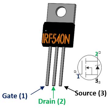
Useful Steps
1) Solder the LM358 IC on the Veroboard. After that, solder the fixed ends of a 10K pot with pin 4 & pin 8 of the IC.
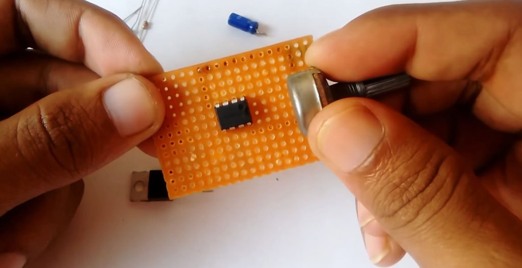
2) Solder a 1K resistor between pin 3 of the LM358 & the wiper pin of the 10K pot.
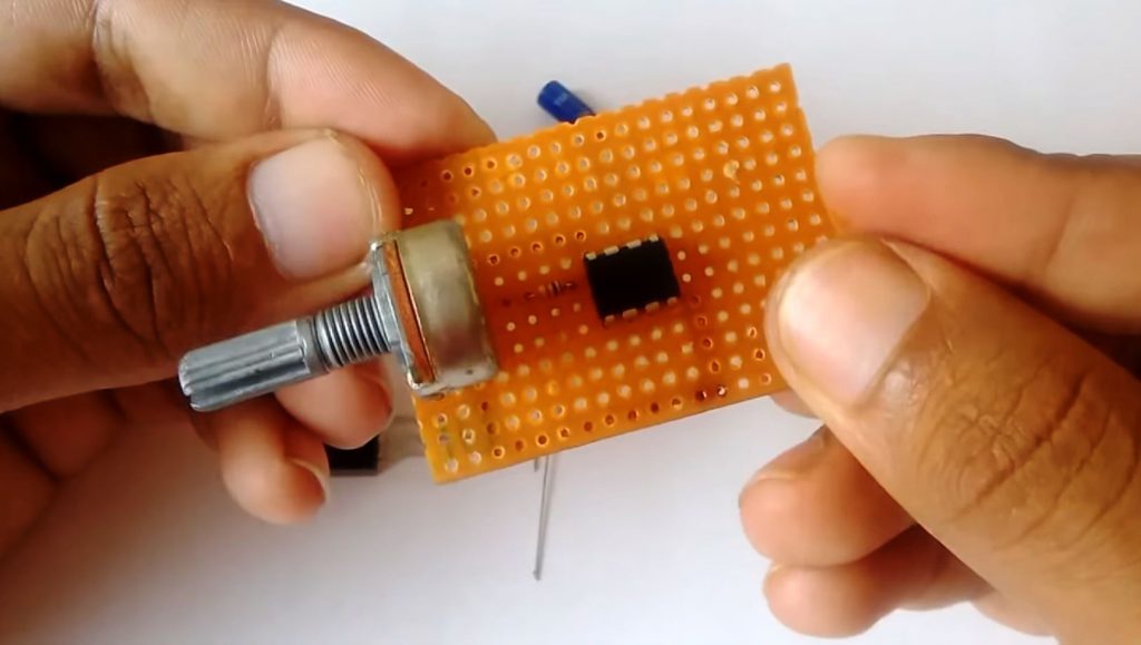
3) After that, Solder the +ve terminal of the 0.1uF capacitor with pin 2 of the IC & -ve terminal to pin 4 of the IC.
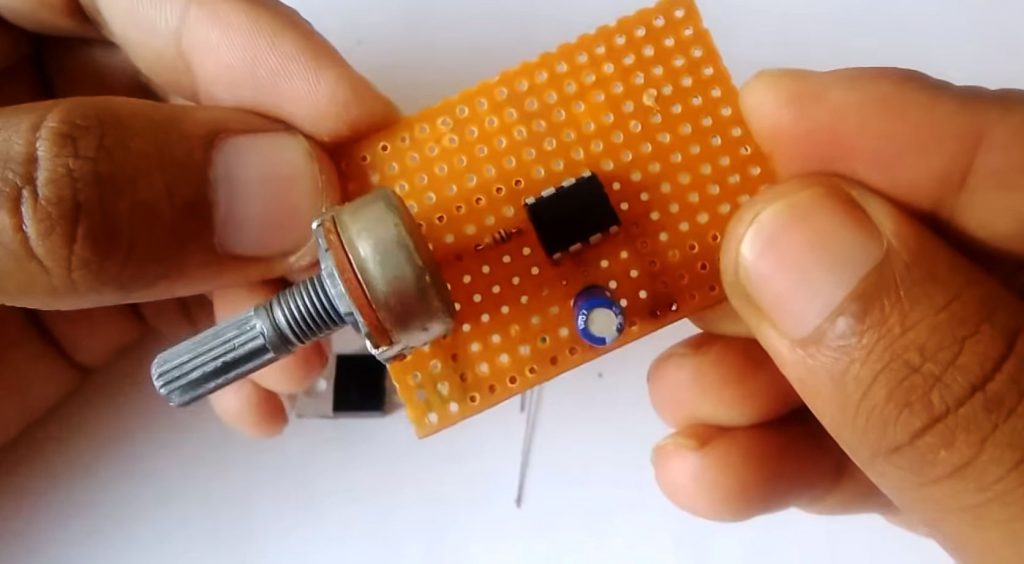
4) After that, solder a 1K resistor with the gate pin of the IRF540 MOSFET.
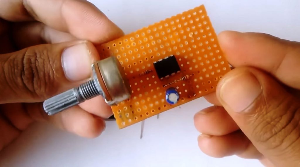
5) Now solder a 10K resistor between pin 1 & 2 of the IC. After that, solder a 47K resistor between pin 1 and pin 3 of the IC.
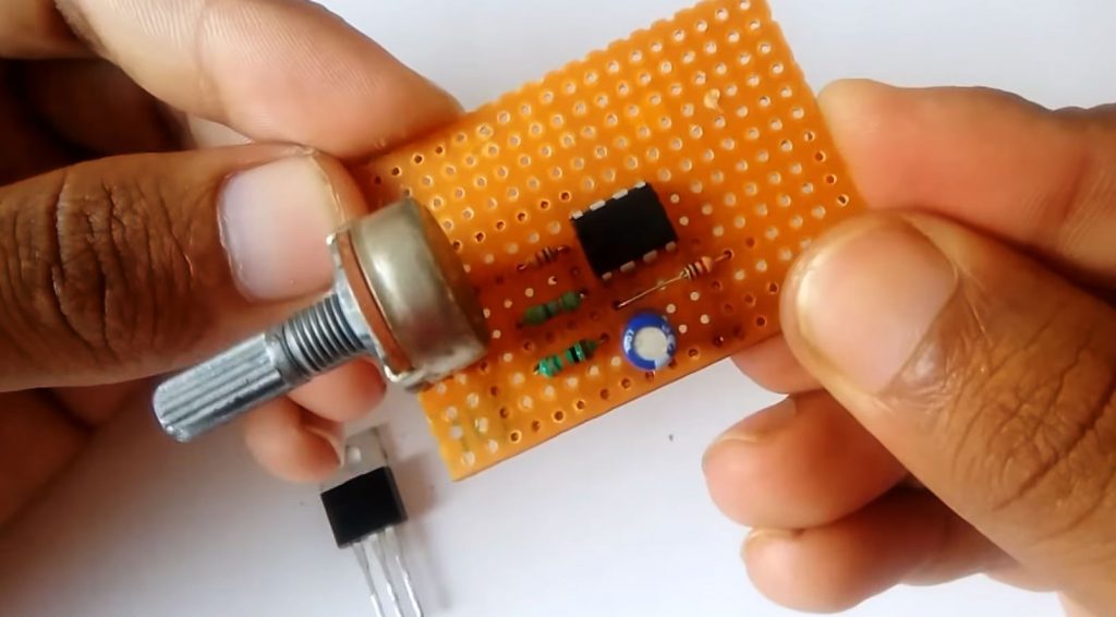
6) After that, solder the source terminal of the IRF540 MOSFET with pin 4 of the IC.
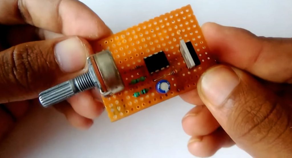
7) Solder the input & output terminal block connectors on the veroboard.
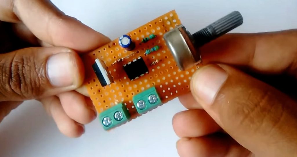
8) Power up and test the circuit using a 9V Battery.

Circuit Diagram For PWM Signal Generator
Working Explanation
The working of this is circuit can be followed by simply understanding the operation of the LM358 Op-Amp. Here we are using the LM358 Op-Amp in Astable multivibrator mode to produce a free running square wave signal. Here, an RC circuit is connected across the output Pin no. 3 of the LM358 op-amp. So that the charging/discharging of the 0.1uF capacitor can be used to create a free-running square signal continuously. You can adjust the duty cycle (%) of the PWM square signal using the 10K preset pot, this will define how fast the switching will take place.
The RC square wave output of the Op-Amp IC serves as the control signal to the gate terminal of the IRF540 power MOSFET. The drain output of which is connected to a DC motor, allowing it to be driven at a high current. If you are going to use this circuit for longer duration, use a heat sink with IRF540 MOSFET to prevent from getting damaged due to excess thermal dissipation
Applications
- Used in Dimmer circuits for lighting fixtures.
- Also used in controlling the speed of DC Motors.
- Controlling the brightness of Monitor Displays.
See Also: How to Create 12v Power Bank | How to setup WiFi on Raspberry Pi 3? | Bike Turning Signal Circuit


